Semiconductor Fab Chemical Monitoring

    Categories Liquid & Gas Analysis, Semiconductor

    Concentration monitor DCM-10 for semiconductor wet chemicals control
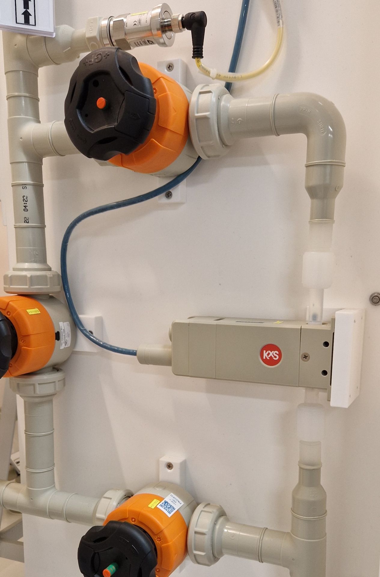
    Brand : KXS

    • Description

    When it comes to balancing cost, speed, and accuracy in semicon chemical concentration measurements throughout the fab distribution chain, in-situ refractive index has become the industry standard.

      KxS semiconductor DCM-10 fab chemical monitor is expertly designed to:

    • Define incoming delivery clean chemical concentration and raw CMP slurry density.
    • Achieve and ensure precise H2O2 concentration and DI water dilutions in colloidal silica-type CMP slurries used in copper, tungsten, and interlayer dielectric planarization applications.
    • Correlate concentration measurements with wafer etch rates (ER) in processes such as buffered oxide etch (BOE).
    • Optimize the bath life of post-etch residue removers like EKC265™ in wet strip spinning tools.

      Our semiconductor fab chemical monitor is ideal for a variety of applications, including:

    • Chemical blend checksum of SC-1, SC-2
    • Hard mask etching with NH3 water mixes
    • Silicon wet etch with 50% KOH
    • Titanium etch with H2SO4:HNO3:H3PO4 mixes
    • Back side poly etch with HF:HNO3 mixtures
    • Post-CMP cleans with various mixtures

      Our technology is capable of monitoring a wide range of critical semiconductor chemicals, including but not limited to:

    • Hydrogen peroxide (H2O2)
    • Ammonium hydroxide (NH3 water)
    • Dilute hydrofluoric acid (HF)
    • Phosphoric acid (H3PO4)
    • Hydrochloric acid (HCl)
    • Sodium hydroxide (NaOH)
    • Sulfuric acid (H2SO4)
    • N-methyl pyrrolidone (NMP)
    • Tetramethylammonium hydroxide (TMAH)
    • Iso-propyl alcohol (IPA)
    • Potassium hydroxide (KOH)
    • Nitric acid (HNO3)
    • Polyethylene glycol (PEG)
    • Citric acid (C6H8O7)
    • Acetic acid (CH3COOH)

    Experience unparalleled precision and efficiency in your chemical monitoring processes with KxS Technologies' advanced solutions and expertise.

    Introducing the KxS semiconductor monitor DCM-10, a cutting-edge optical refractometer designed for real-time monitoring of wet chemicals in almost all processing steps that involve wafer processing with liquid chemicals or mixtures. The DCM-10 is renowned for its high accuracy and reliability, making it an essential concentration monitoring tool for incoming chemical check, wafer cleaning, chemical etching and chemical mechanical planarization (CMP).

    Advanced functionality

    The DCM-10 operates with a 24 VDC input power supply and offers flexible communication options, including analog (4-20 mA) and digital (Modbus TCP). When using the analog signal, the digital port serves as a service port for configuration and diagnostics via a computer web browser, external display, or mobile device. All port options can be utilized simultaneously, providing seamless integration and monitoring capabilities.

    Precision and calibration

    Factory calibrated for refractive index measurements, the DCM-10 displays temperature-compensated concentration units in % by weight or g/cm³. This ensures accurate and consistent monitoring of chemical concentrations, critical for maintaining process integrity and quality.

      Key features

    • True standalone operation: All measurement functions contained within the sensor, eliminating the need for an external transmitter.
    • Extra small footprint design: The compact sensor and flow are ideal and fit into fab tools and benches.
    • Excellent flow properties: True full bore; Optimized laminar flow pattern with minimal shear force on liquid (Patent pending).
    • Easy installation: Connects with process line sizes of ¼, ⅜, ½, ¾, and 1 inch, using standard fittings.
    • Dual-body construction: Optical components remain intact even if the flow cell is removed, ensuring consistent performance.
    • Material compatibility: Materials designed to withstand the demanding conditions of semiconductor processing in the facilities and cleanroom environments.

    In the fast-evolving semiconductor industry, precision in chemical concentration measurement is critical to ensuring process stability, yield optimization, and cost efficiency.

    KxS Technologies’ in-situ refractive index measurement technology balances cost, speed and accuracy in providing real-time monitoring to maintain chemical integrity, reduce waste, and enhance process control throughout the fab distribution chain.

    Typical application areas

    1. Chemical blend checksum for SC-1 and SC-2

    Our sensors are used in blender systems achieving the correct concentration of constituents in SC-1 and SC-2 cleaning solutions being essential for effective particle removal and surface preparation.

    2. Onsite production of high-purity NH₃(aq) ammonium hydroxide

    Along with an increasingly complex chemical supply chain new ways in generating chemicals onsite are advocated. Blenders generating bulk 29% NH₃(aq) from ammonia gas and water adopt the DCM-10 refractometer for ensuring the formation of ammonia liquid to its bulk concentration. Refractive index is uniquely a good match in the entire ammonia concentration range 0-30%wt.

    3. Silicon wet etch with 50% KOH

    Anisotropic wet etching of silicon with 50% potassium hydroxide (KOH) demands precise control to achieve smooth, accurate etching profiles, particularly in MEMS and deep etch applications.

    4. Titanium etch with H₂SO₄:HNO₃:H₃PO₄ mixes

    Titanium etching requires balanced acid blends of sulfuric acid (H₂SO₄), nitric acid (HNO₃), and phosphoric acid (H₃PO₄) to ensure efficient material removal while minimizing defects and over-etching. Our technology provides continuous monitoring for optimized concentration levels.

    5. Backside poly etch with HF:HNO₃ mixtures

    The selective etching of polycrystalline silicon on wafer back sides requires precise HF:HNO₃ concentration control to maintain process uniformity.

    6. Post-CMP cleans with various mixtures

    Chemical mechanical planarization (CMP) introduces contaminants that must be effectively removed using post-CMP cleaning solutions. Our sensors optimize cleaning bath life and ensure proper chemical balance for consistent wafer surface quality.

      Why choose KxS for semiconductor applications?

    • Real-time chemical monitoring – Instant concentration verification for process stability.
    • Improved process yield – Reduce chemical waste and extend bath life.
    • Cost and efficiency optimization – Minimize overuse of chemicals and improve ROI.
    • Industry-proven reliability – Trusted by leading semiconductor fabs worldwide.

    Brochures

    Download

    Manuals

    Download

    Certificates

    DNV Management System Certificate ISO 9001:2015

    Download

    DCM-10 ATEX certificate II 2/3G Ex ec mc IIC T4 Gb/Gc

    Download

    DCM-10 IECEx certiicate II 2/3G Ex ec mc IIC T4 Gb/Gc

    Download

    Technical Notes

    Download

    Applications

    KxS Application Insights Semiconductor CMP slurry Insights

    Download

    Slurry Delivery Systems Defining Incoming CMP Slurry Density and Achieving Target Process Conctration Driven by Inline Metrology Unify CMP Engineers - ICPT_2022

    Download

    Inline Refractive Index-based Slurry Density Monitoring to Optimize Raw CMP Slurry Container Dispersion - ICPT_2023

    Download